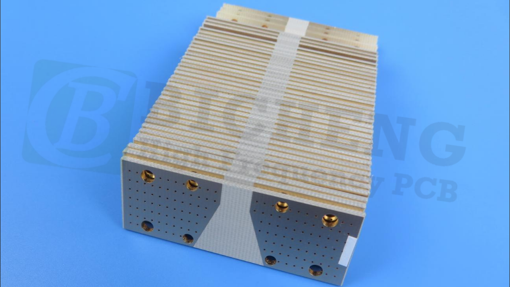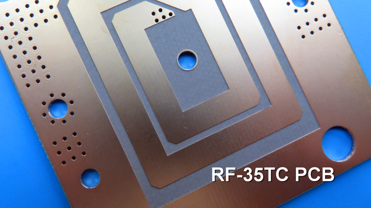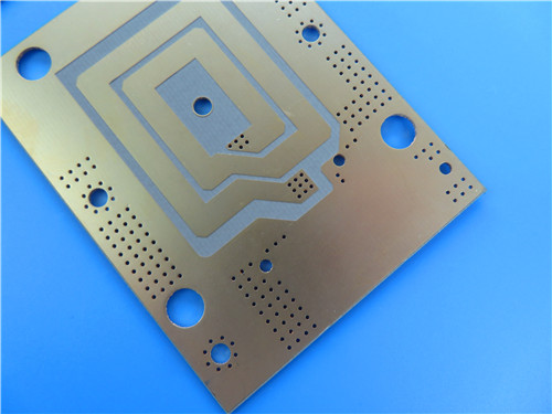
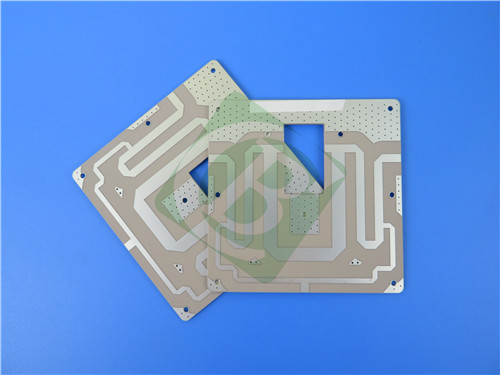
RF-35 2-Layer PCB Optimal Solution for RF and Microwave Circuits1.Product Introduction Taconic's RF-35 organic-ceramic laminate combines woven glass reinforcement with advanced ceramic fill technology to deliver exceptional high-frequency performance. This cost-effective 2-layer PCB material features excellent peel strength, ultra-low moisture absorption, and minimal phase shift - making it ideal for commercial microwave applications requiring reliable signal integrity. 2.Key Technical Features Stable Dielectric Properties: 3.PCB Construction Specifications
4.PCB Stackup: 2-layer rigid PCB Copper_layer_1 - 35 μm 5.PCB Statistics: Components: 18 6.Performance Advantages Cost-competitive alternative for RF designs 7.Primary Applications Cellular infrastructure power amplifiers 8.Quality Assurance IPC-Class 2 standards compliance |
Get a Quick Quote
Fill in the form below and our engineers will reply within 24 hours with technical specifications and pricing for RF-35 2-Layer PCB Optimal Solution for RF and Microwave Circuits.
.jpg)
.jpg)
.jpg)
.jpg)
.jpg)
.jpg)
.jpg)
.jpg)